What is a Silicon Carbide Wafer?
- hope
- 2025-02-05 16:31:30
Introduction to Silicon Carbide Wafers
A silicon carbide wafer is a thin, flat, disk-shaped piece of silicon carbide (SiC) that serves as a foundation for manufacturing a variety of semiconductor devices. Silicon carbide, a compound of silicon and carbon, exhibits exceptional properties, making it a vital material in high-performance electronics. Its inherent characteristics, such as high thermal conductivity, high voltage tolerance, and robust physical structure, have made SiC wafers indispensable in industries such as power electronics, automotive, renewable energy, and more.
What is Silicon Carbide?
Silicon carbide (SiC) is a compound composed of equal parts of silicon and carbon. Unlike pure silicon, which is widely used in semiconductor manufacturing, SiC is known for its superior properties that make it suitable for extreme environments. SiC’s wide bandgap allows it to perform under high temperatures, high voltages, and harsh conditions that would cause conventional silicon materials to fail. These attributes make silicon carbide an attractive choice for advanced semiconductor applications.
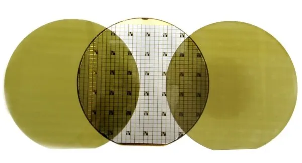
Manufacturing of Silicon Carbide Wafers
The production of silicon carbide wafers involves several highly advanced and meticulous steps. The process begins with growing high-quality SiC crystals, typically through a method called sublimation. Once the crystals are grown, they are sliced into thin wafers, usually measuring from 2 inches to 6 inches in diameter, though larger sizes are possible. The surface of these wafers is then polished to perfection, ensuring they meet the stringent requirements for semiconductor fabrication.
- Sublimation: In this process, silicon carbide crystals are grown in a high-temperature furnace using a method called physical vapor transport (PVT), which ensures high purity and crystalline quality.
- Wafer Cutting: After the crystals have been grown, they are sliced into thin wafers with the aid of precision equipment to achieve the desired thickness and diameter.
- Polishing: Each wafer undergoes a polishing process that removes surface imperfections, leaving a smooth and flat surface that is essential for semiconductor fabrication.
Advantages of Silicon Carbide Wafers
Silicon carbide wafers offer numerous advantages over traditional silicon wafers, especially when it comes to high-power and high-temperature applications. The material's inherent properties are pivotal in enhancing the performance of electronic devices and improving energy efficiency.
- High Thermal Conductivity: SiC wafers are highly efficient at dissipating heat, which is crucial for high-power applications. This reduces the risk of overheating and ensures long-term reliability.
- Wide Bandgap: With a bandgap of around 3.26 eV, silicon carbide allows for faster switching speeds and the ability to handle higher voltages, enabling the development of more efficient power devices.
- High Voltage Tolerance: SiC wafers can operate at much higher voltages than traditional silicon wafers, making them ideal for use in power electronics, electric vehicles, and renewable energy systems.
- Enhanced Efficiency: Devices made from SiC wafers are more energy-efficient, as they experience less energy loss compared to silicon-based devices. This is particularly important in industries where power conversion efficiency is critical.
Applications of Silicon Carbide Wafers
Silicon carbide wafers are used in a variety of industries, particularly in fields where high efficiency, power handling, and thermal performance are required. Some of the primary applications include:
- Power Electronics: SiC wafers are used to produce diodes, transistors, and other power devices, which are integral components in power electronics. These devices are used in power inverters, motor drives, and energy-efficient systems.
- Electric Vehicles (EVs): The automotive industry, particularly the electric vehicle sector, greatly benefits from SiC wafers. SiC-based power devices help increase the driving range and reduce charging times for EVs.
- Renewable Energy: Solar inverters, wind turbines, and other renewable energy systems rely on SiC-based power devices to efficiently convert energy, improving the overall performance and sustainability of these technologies.
- High-Frequency Applications: SiC wafers are also used in high-frequency devices like RF amplifiers and radar systems, where their ability to handle high-power signals makes them more effective than traditional semiconductor materials.
- Aerospace and Defense: Due to their high-temperature and radiation resistance, SiC wafers are used in aerospace applications and military technologies, where reliability in harsh environments is essential.
The Future of Silicon Carbide Wafers
The demand for silicon carbide wafers is expected to increase rapidly in the coming years, driven by the growing need for more efficient and reliable power electronics. As industries continue to prioritize energy efficiency and environmental sustainability, SiC wafers will play a critical role in the development of next-generation technologies.
Advancements in manufacturing techniques, including the ability to produce larger wafers at lower costs, will further expand the use of silicon carbide wafers in mainstream applications. The rise of electric vehicles, renewable energy systems, and energy-efficient technologies will continue to fuel the adoption of SiC-based devices, ensuring the material's place at the forefront of the semiconductor industry.
Conclusion
In conclusion, a silicon carbide wafer is a fundamental material in the production of high-performance electronic devices. Offering a variety of advantages such as high thermal conductivity, high voltage tolerance, and exceptional efficiency, SiC wafers are transforming industries ranging from power electronics to automotive and renewable energy. With the continued growth of these sectors, silicon carbide will remain an integral part of technological advancements, helping create more efficient, sustainable, and reliable electronic devices for the future.